- 易迪拓培训,专注于微波、射频、天线设计工程师的培养
Re: PIN diode in CST MWS
I am using CST Studio Suite 2011 software for designing the Fractral Tree antenna using PIN Diode but I don't know how to use pin diode in CST Studio Suite 2011 software.
So please help me If you have any pdf or step by step instruction or demo project regarding above topic.
Thank you Sir...!
Hi all,
I've had a couple of PM's seeking clarification about my flippant instruction:
...so I thought I'd elaborate a little :)
As you undoubtedly know, the VNA (network analyser) applies small AC excitations to each of its test ports and measures the energy 'scattered' back (and to its other ports, if applicable.) In the case where the DUT (device under test) is an active component, it's often desired to apply a DC bias in addition to the AC test signal in order to a) bias the component into an active region of interest (i.e. make it work), and b) examine how the scattering parameters change as the bias is changed.
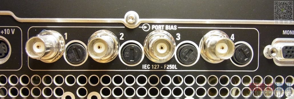
While you *can* add external bias circuitry (as would be required when the device is actually embedded into a circuit), these networks present their own parasitic effects and can obscure detailed, isolated study of the active DUT. An example external bias network is the classic "Bias-T" (http://en.wikipedia.org/wiki/Bias_tee). Every VNA I've ever used offers a nifty alternative though... on the back panel of the R&S ZVB on my desk there are 4 BNC connectors:

If you apply a DC voltage to these connectors, it will be supplied to the corresponding test port of the instrument (which you"ve coupled directly to your DUT) *without affecting the measurement*! Cool, eh?
The limitations of the bias voltages/currents will be listed in the VNA's manual so check the specifications first, but I've found them to be more than adequate for small-signal LNA to low-power driver amplifier characterisation. I'd never noticed the fuses there before though... undoubtedly a sensible addition by Rohde & Schwarz :)
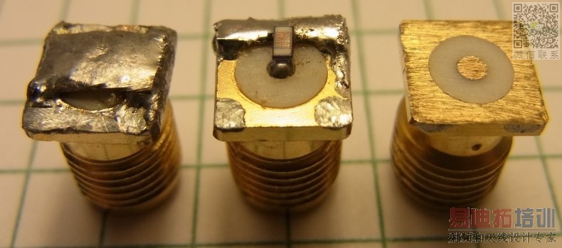
That's how you apply the PIN diode bias. To test the device itself, solder it across the back of an SMA connector, as illustrated in the following photo:

This photo shows three connectors I used when previously measuring the parasitics of the 43nH 0603 inductor DUT in the centre. (No comments on my soldering please ;)
The other two [identical] connectors are approximations to a "short" and an "open". They are useful to guide you in the adjustment of the instrument's reference plane from that defined during calibration to the plane [position] where your DUT lies on an otherwise identical connector. Sometimes (as my R&S ZVB does) the VNA will incorporate a "fixture compensation" feature which allows you to use these 'short/open terminations' to nudge the internal calibration derived from the precision calibration kit. Alternatively, you can manually adjust the reference plane with each of these terminations connected until the instrument measures sensible impedances (i.e. low for the short and high for the open) for each.
After adjusting the reference plane, you can connect your DUT and apply the desired bias via the rear panel connectors. The instrument will now directly measure the characteristics of your DUT at your desired operating point!
From here you can extract the RLC equivalent parameters for your test frequencies. There are numerous ways to do this, and they range in complexity from simple (i.e. choose a series RLC combination to equal the measured impedance) to complex when a higher order model or broad-band characterisation is required. I recall seeing a number of MATLAB tools in the past, hit Google.
Good luck!
申明:网友回复良莠不齐,仅供参考。如需专业解答,请学习易迪拓培训专家讲授的CST视频培训教程。
上一篇:How can I get the Polarization of the Electric field in CST?
下一篇:template based postprocessing of CST

