- 易迪拓培训,专注于微波、射频、天线设计工程师的培养
[CST] How to simulate an ISS ( impedance standard substrate )
录入:edatop.com 点击:
Dear all,
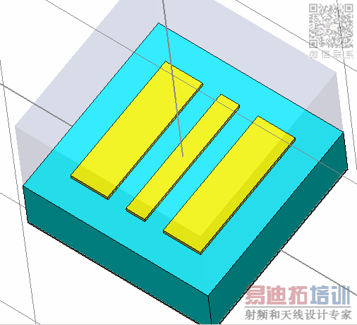
I'm tryng to simulate a CST structure like the one you can see in the picture. The structure represent the Open standard realized with alumina on a silicon substrate.
The three pads represents the landing pads of a typical ground-signal-ground probe.
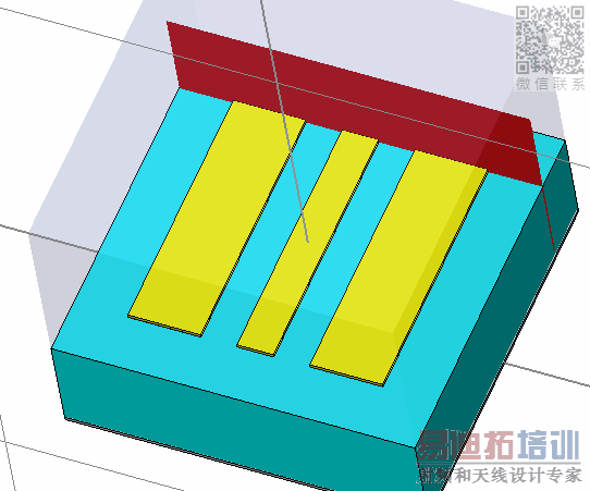
The problem is how to simulate them. Do you suggest to use a waveguide port ( as shown in the second picture ) or three lumped port, one on each pad?
Thank you in advance,
V.M.
Vsl,
Per the CST manual, if there are 3 or more conductors in proximity it is recommended that you use a multipin waveguide port. I would recommend reading this section of the manual, it isn't that dense. It is easy to find by clicking on "help" while you are in the waveguide port creation menu.
申明:网友回复良莠不齐,仅供参考。如需专业解答,请学习易迪拓培训专家讲授的CST视频培训教程。
上一篇:CST - Meshing doubt
下一篇:farfieldplot cst


